
Semiconductors • Industrial Policy
The AI Chip War Enters Its Infrastructure Phase: Beyond the GPU Scramble
The strategic commodity is no longer a single processor. It is an entire production system spanning extreme-ultraviolet lithography, advanced packaging, memory stacks, and dedicated electric power grids.

On September 14, 2026, two disparate announcements illustrated the structural transition underway in computing hardware. In Beijing, state media condemned Western calls for tighter semiconductor controls as part of a geopolitical containment effort. In Europe, ASML disclosed that its extreme-ultraviolet (EUV) lithography systems, priced at roughly 200 million dollars apiece, were virtually sold out through 2027, while leading foundries committed tens of billions to next-generation High-NA systems costing approximately 400 million dollars each. The geopolitical dispute and the manufacturing bottleneck are, in reality, facets of the same industrial transformation.
The initial phase of the artificial intelligence boom was commonly characterized as a straightforward race to procure Nvidia graphics processing units. That model is now obsolete. The decisive commodity is no longer an isolated processor. It is an integrated production system: leading-edge fabrication, photolithography tools, high-bandwidth memory (HBM), advanced packaging, optical interconnects, dedicated high-voltage electricity, and specialized materials. Whoever assembles this entire stack at scale commands something far greater than fast silicon: the industrial capacity to convert electric power into machine intelligence.
This shift reframes the meaning of technological advantage. Export controls can restrict particular chip shipments. Government subsidies can relocate individual fabrication facilities. Neither action alone builds an autonomous semiconductor ecosystem. By late 2026, the strategic question confronting the United States, China, Europe, Taiwan, Japan, and South Korea is no longer who owns the fastest GPU. It is who governs the physical bottlenecks that make computing clusters possible.
"Counting GPUs to gauge artificial intelligence dominance is like measuring twentieth-century military aviation purely by counting engines while disregarding airframes, fuel refineries, and radar networks. Compute is an interconnected industrial machine."
The Contest Beneath the Accelerator
The financial scale of modern AI explains why supply chain nodes have become prime geopolitical territory. Nvidia reported 96.2 billion dollars in revenue for its second quarter ending July 2026, more than doubling its revenue from the previous year. Its Data Centre division alone accounted for 89 billion dollars, surging 117 percent year on year. Crucially, Nvidia's near-term guidance forecast 108 billion dollars while explicitly assuming zero data-center compute sales to China. The global market outside China has expanded so aggressively that the dominant vendor can generate over 100 billion dollars in quarterly revenue without Chinese server sales.
Yet Nvidia occupies only the design and software layer of a vast industrial hierarchy. Taiwan Semiconductor Manufacturing Company (TSMC) reported second-quarter 2026 revenue of 40.2 billion dollars, boasting a gross margin of 67.7 percent and an operating margin of 60.3 percent. TSMC's manufacturing footprint is expanding internationally: its Arizona investment programme has grown from an initial 12-billion-dollar project into a stated 265-billion-dollar complex encompassing six logic fabs, two advanced packaging facilities, and an advanced research center.
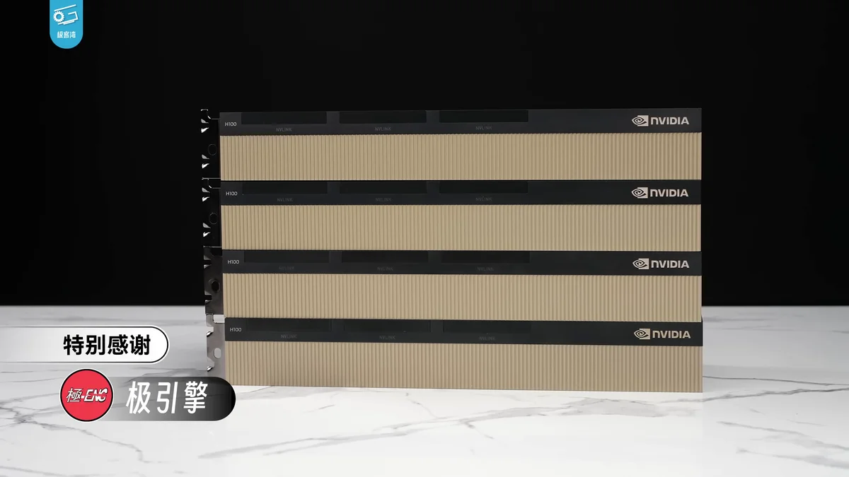
This reality dismantles the simplistic political rhetoric of quick national reshoring. A modern fabrication plant depends on equipment from hundreds of specialized global suppliers, ultra-pure chemicals, synthetic gases, photomasks, electronic design automation software, and precision packaging. AI accelerators compound this reliance because modern chips combine multiple silicon dies and memory stacks rather than relying on a single monolithic piece of silicon.
TSMC's CoWoS (Chip-on-Wafer-on-Substrate) packaging roadmap demonstrates where competition is heading. Having deployed 5.5-reticle-size packages in production, TSMC plans a 14-reticle variant for 2028 capable of integrating roughly ten compute dies alongside twenty high-bandwidth memory stacks. The fundamental unit of hardware competition has transitioned from the individual transistor to an integrated multi-die system.
| Supply Chain Layer | Primary Global Anchors | Key Industrial Constraint | Strategic Substitutability |
|---|---|---|---|
| Photolithography | ASML (Netherlands) | EUV optics, High-NA tooling capacity | Near zero (commercial monopoly) |
| Leading-Edge Foundry | TSMC (Taiwan, US, Japan) | Yield rates at 3nm/2nm, multi-year fab ramp cycles | Very low (requires 5-7 years) |
| High-Bandwidth Memory | SK Hynix, Samsung, Micron | Through-silicon via (TSV) yield, thermal dissipation | Extremely constrained globally |
| Advanced Packaging | TSMC CoWoS, Amkor, ASE | Interposer scaling, substrate manufacturing | High technical barrier |
| Electric Grid Capacity | Regional utilities (PJM, ERCOT, State Grid) | Substation transformers, transmission permits | Locally non-substitutable |
Lithography as the Decisive Chokepoint
No enterprise illustrates supply chain concentration more starkly than ASML. In September 2026, the company's existing low-NA EUV machinery was fully committed through 2027, with full-year revenues projected between 43 and 45 billion euros. The newest High-NA EUV tools, capable of etching features 40 percent smaller than standard EUV, have begun initial customer integration across Intel, TSMC, Samsung, and SK Hynix.
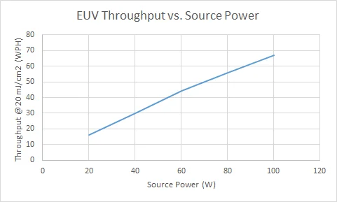
Frontier lithography is embodied physics: extreme ultraviolet light generated by vaporizing microscopic molten tin droplets with high-power carbon dioxide lasers fifty thousand times per second. It cannot be reproduced simply by appropriating venture capital or government grants. ASML's planned manufacturing expansion (increasing annual low-NA EUV machine production from 65 units to roughly 85 units by 2028) defines the ultimate physical limit on how many advanced wafers the entire planet can fabricate.
Export Policy as Active Market Architecture
United States semiconductor policy has evolved from blunt trade embargoes into an active framework of market design. In January 2026, the Bureau of Industry and Security (BIS) revised export review guidelines for processors including Nvidia's H200 and AMD's MI325X. Instead of presumptive denials, BIS instituted conditional case-by-case reviews requiring end-user screening, independent testing, and strict quotas to ensure foreign allocations do not deplete domestic capacity.
This followed the rescission of the 2025 AI Diffusion Rule, which had attempted to divide world markets into rigid geopolitical tiers. Policymakers recognized that restrictions which are excessively punitive risk pushing allied partners toward independent ecosystems and depriving Western semiconductor champions of the global revenues required to fund subsequent research cycles.
Simultaneously, China's domestic ecosystem is organizing around the blockade. Hua Hong's Huali Microelectronics has introduced domestic 7-nanometer wafer processing, joining SMIC in sub-10nm capability. Chinese memory producers CXMT and YMTC have been directed to prioritize domestic AI clients. An academic study published in mid-2026 demonstrated that while export controls heightened short-term friction for Chinese developers, they significantly accelerated domestic open-source contributions and algorithmic optimizations.
The Energy Frontier
The semiconductor debate has historically treated electric power as a mere operational utility. In 2026, electricity is recognized as a strategic manufacturing input equivalent to silicon wafers.
The International Energy Agency forecasts global data-center electricity consumption will surge from 485 terawatt-hours in 2025 to 950 TWh by 2030, accounting for 3 percent of worldwide energy demand. In the United States, Lawrence Berkeley National Laboratory estimates data centers could consume up to 11.8 percent of total national electricity by 2030. In South Korea, energy officials disclosed that planned semiconductor cluster expansions will require between 25 and 30 gigawatts of additional generation capacity, equivalent to the entire output of twenty nuclear reactors.
This convergence alters national industrial strategy. A state may secure silicon allocations, fiber optic connectivity, and server racks, but remain unable to deploy frontier computing because utility substations, transmission rights, and power permits require five to seven years to deliver.
The Strategic Verdict
The decisive technological advantage of the late 2020s will not belong to the nation that hoards the largest stockpile of individual GPUs. It will belong to the coalition that coordinates lithography delivery, foundry yields, high-bandwidth memory allocations, advanced packaging facilities, and gigawatt-scale electrical grids into a continuous, resilient industrial engine.
References & Archival Documentation
- • ASML Holding N.V., Q2 2026 Financial Results and Lithography Capacity Planning, July 2026.
- • Taiwan Semiconductor Manufacturing Co., 2026 North America Technology Symposium & Packaging Roadmap.
- • Nvidia Corporation, Form 10-Q Quarterly Filing, Data Center Revenue Segment, August 2026.
- • US Bureau of Industry and Security (BIS), Semiconductor Export Licensing Guidance Revision, January 2026.
- • International Energy Agency (IEA), Energy and AI: Global Infrastructure Demand Projections, 2026.
- • Lawrence Berkeley National Laboratory, United States Data Center Energy Usage Report, June 2026.